

Which Cameras Use Ccd Sensor

A specially developed CCD in a wire-bonded package used for ultraviolet imaging
A charge-coupled device (CCD) is an integrated circuit containing an array of linked, or coupled, capacitors. Nether the control of an external circuit, each capacitor tin transfer its electric charge to a neighboring capacitor. CCD sensors are a major engineering used in digital imaging.
In a CCD prototype sensor, pixels are represented by p-doped metal–oxide–semiconductor (MOS) capacitors. These MOS capacitors, the basic building blocks of a CCD,[ane] are biased higher up the threshold for inversion when epitome acquisition begins, allowing the conversion of incoming photons into electron charges at the semiconductor-oxide interface; the CCD is then used to read out these charges. Although CCDs are not the but engineering science to allow for light detection, CCD image sensors are widely used in professional, medical, and scientific applications where loftier-quality image information are required. In applications with less exacting quality demands, such as consumer and professional digital cameras, active pixel sensors, likewise known as CMOS sensors (complementary MOS sensors), are generally used. However, the large quality advantage CCDs enjoyed early on has narrowed over time and since the tardily 2010s CMOS sensors are the dominant engineering, having largely if not completely replaced CCD paradigm sensors.
History [edit]
The basis for the CCD is the metal–oxide–semiconductor (MOS) structure,[2] with MOS capacitors being the basic building blocks of a CCD,[1] [3] and a depleted MOS construction used equally the photodetector in early CCD devices.[two] [4]
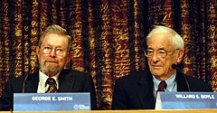
In the late 1960s, Willard Boyle and George E. Smith at Bell Labs were researching MOS engineering science while working on semiconductor bubble memory. They realized that an electrical charge was the analogy of the magnetic chimera and that it could be stored on a tiny MOS capacitor. As it was fairly straightforward to fabricate a serial of MOS capacitors in a row, they connected a suitable voltage to them so that the charge could be stepped along from ane to the adjacent.[3] This led to the invention of the charge-coupled device by Boyle and Smith in 1969. They conceived of the pattern of what they termed, in their notebook, "Charge 'Bubble' Devices".[5] [6]
The initial newspaper describing the concept in Apr 1970 listed possible uses every bit memory, a filibuster line, and an imaging device.[7] The device could also be used as a shift register. The essence of the blueprint was the ability to transfer accuse forth the surface of a semiconductor from one storage capacitor to the next. The concept was similar in principle to the bucket-brigade device (BBD), which was developed at Philips Research Labs during the tardily 1960s.
The showtime experimental device demonstrating the principle was a row of closely spaced metal squares on an oxidized silicon surface electrically accessed by wire bonds. It was demonstrated past Gil Amelio, Michael Francis Tompsett and George Smith in Apr 1970.[8] This was the offset experimental application of the CCD in paradigm sensor technology, and used a depleted MOS structure as the photodetector.[2] The first patent (U.S. Patent iv,085,456) on the application of CCDs to imaging was assigned to Tompsett, who filed the application in 1971.[9]
The first working CCD made with integrated circuit applied science was a uncomplicated 8-chip shift annals, reported by Tompsett, Amelio and Smith in August 1970.[10] This device had input and output circuits and was used to demonstrate its apply as a shift register and as a crude eight pixel linear imaging device. Development of the device progressed at a rapid rate. By 1971, Bong researchers led by Michael Tompsett were able to capture images with elementary linear devices.[11] Several companies, including Fairchild Semiconductor, RCA and Texas Instruments, picked up on the invention and began development programs. Fairchild's effort, led by ex-Bell researcher Gil Amelio, was the kickoff with commercial devices, and by 1974 had a linear 500-element device and a two-D 100 × 100 pixel device. Steven Sasson, an electrical engineer working for Kodak, invented the kickoff digital still camera using a Fairchild 100 × 100 CCD in 1975.[12]
The interline transfer (ILT) CCD device was proposed by L. Walsh and R. Dyck at Fairchild in 1973 to reduce smear and eliminate a mechanical shutter. To farther reduce smear from bright light sources, the frame-interline-transfer (FIT) CCD architecture was developed past Chiliad. Horii, T. Kuroda and T. Kunii at Matsushita (now Panasonic) in 1981.[2]
The first KH-11 KENNEN reconnaissance satellite equipped with charge-coupled device assortment (800 × 800 pixels)[13] engineering science for imaging was launched in December 1976.[14] Nether the leadership of Kazuo Iwama, Sony started a large development endeavor on CCDs involving a significant investment. Eventually, Sony managed to mass-produce CCDs for their camcorders. Before this happened, Iwama died in August 1982; subsequently, a CCD bit was placed on his tombstone to acknowledge his contribution.[15] The first mass-produced consumer CCD video photographic camera, the CCD-G5, was released past Sony in 1983, based on a prototype developed by Yoshiaki Hagiwara in 1981.[xvi]
Early on CCD sensors suffered from shutter lag. This was largely resolved with the invention of the pinned photodiode (PPD).[two] It was invented by Nobukazu Teranishi, Hiromitsu Shiraki and Yasuo Ishihara at NEC in 1980.[ii] [17] They recognized that lag tin can be eliminated if the signal carriers could be transferred from the photodiode to the CCD. This led to their invention of the pinned photodiode, a photodetector structure with depression lag, low noise, high quantum efficiency and low dark current.[2] Information technology was offset publicly reported by Teranishi and Ishihara with A. Kohono, E. Oda and One thousand. Arai in 1982, with the improver of an anti-blooming structure.[2] [18] The new photodetector structure invented at NEC was given the proper noun "pinned photodiode" (PPD) past B.C. Burkey at Kodak in 1984. In 1987, the PPD began to exist incorporated into most CCD devices, becoming a fixture in consumer electronic video cameras and and so digital notwithstanding cameras. Since then, the PPD has been used in nearly all CCD sensors and and so CMOS sensors.[2]
In January 2006, Boyle and Smith were awarded the National Academy of Engineering Charles Stark Draper Prize,[19] and in 2009 they were awarded the Nobel Prize for Physics[20] for their invention of the CCD concept. Michael Tompsett was awarded the 2010 National Medal of Applied science and Innovation, for pioneering work and electronic technologies including the blueprint and development of the starting time CCD imagers. He was also awarded the 2012 IEEE Edison Medal for "pioneering contributions to imaging devices including CCD Imagers, cameras and thermal imagers".
Basics of operation [edit]
![]()
The charge packets (electrons, blue) are collected in potential wells (yellow) created by applying positive voltage at the gate electrodes (G). Applying positive voltage to the gate electrode in the right sequence transfers the accuse packets.
In a CCD for capturing images, there is a photoactive region (an epitaxial layer of silicon), and a transmission region made out of a shift annals (the CCD, properly speaking).
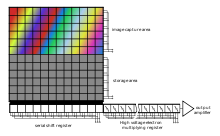
An image is projected through a lens onto the capacitor array (the photoactive region), causing each capacitor to accumulate an electric charge proportional to the light intensity at that location. A one-dimensional assortment, used in line-browse cameras, captures a single slice of the image, whereas a two-dimensional array, used in video and nevertheless cameras, captures a two-dimensional picture corresponding to the scene projected onto the focal plane of the sensor. In one case the assortment has been exposed to the image, a control circuit causes each capacitor to transfer its contents to its neighbor (operating as a shift register). The last capacitor in the assortment dumps its charge into a charge amplifier, which converts the accuse into a voltage. By repeating this process, the controlling circuit converts the entire contents of the array in the semiconductor to a sequence of voltages. In a digital device, these voltages are so sampled, digitized, and ordinarily stored in memory; in an analog device (such as an analog video camera), they are processed into a continuous analog indicate (east.yard. by feeding the output of the charge amplifier into a depression-pass filter), which is and so candy and fed out to other circuits for transmission, recording, or other processing.[21]
Detailed physics of operation [edit]
Charge generation [edit]
Before the MOS capacitors are exposed to light, they are biased into the depletion region; in due north-aqueduct CCDs, the silicon under the bias gate is slightly p-doped or intrinsic. The gate is so biased at a positive potential, above the threshold for potent inversion, which will eventually result in the creation of an n aqueduct below the gate as in a MOSFET. All the same, it takes time to reach this thermal equilibrium: upwardly to hours in loftier-terminate scientific cameras cooled at low temperature.[22] Initially after biasing, the holes are pushed far into the substrate, and no mobile electrons are at or near the surface; the CCD thus operates in a non-equilibrium state called deep depletion.[23] And so, when electron–hole pairs are generated in the depletion region, they are separated by the electric field, the electrons motion toward the surface, and the holes motion toward the substrate. 4 pair-generation processes can be identified:
- photo-generation (upward to 95% of quantum efficiency),
- generation in the depletion region,
- generation at the surface, and
- generation in the neutral bulk.
The concluding iii processes are known as dark-current generation, and add racket to the paradigm; they tin limit the total usable integration time. The aggregating of electrons at or near the surface can keep either until image integration is over and charge begins to be transferred, or thermal equilibrium is reached. In this case, the well is said to be full. The maximum chapters of each well is known as the well depth,[24] typically nearly 105 electrons per pixel.[23]
Design and manufacturing [edit]
The photoactive region of a CCD is, generally, an epitaxial layer of silicon. It is lightly p doped (unremarkably with boron) and is grown upon a substrate material, often p++. In buried-aqueduct devices, the type of blueprint utilized in most modern CCDs, certain areas of the surface of the silicon are ion implanted with phosphorus, giving them an due north-doped designation. This region defines the channel in which the photogenerated charge packets will travel. Simon Sze details the advantages of a cached-channel device:[23]
This sparse layer (= 0.2–0.3 micron) is fully depleted and the accumulated photogenerated accuse is kept away from the surface. This construction has the advantages of college transfer efficiency and lower dark current, from reduced surface recombination. The penalization is smaller charge chapters, by a gene of 2–3 compared to the surface-channel CCD.
The gate oxide, i.eastward. the capacitor dielectric, is grown on top of the epitaxial layer and substrate.
After in the process, polysilicon gates are deposited by chemical vapor degradation, patterned with photolithography, and etched in such a way that the separately phased gates lie perpendicular to the channels. The channels are further defined past utilization of the LOCOS process to produce the channel stop region.
Aqueduct stops are thermally grown oxides that serve to isolate the charge packets in ane column from those in another. These aqueduct stops are produced before the polysilicon gates are, as the LOCOS process utilizes a high-temperature pace that would destroy the gate cloth. The channel stops are parallel to, and sectional of, the aqueduct, or "charge carrying", regions.
Channel stops frequently have a p+ doped region underlying them, providing a further barrier to the electrons in the accuse packets (this give-and-take of the physics of CCD devices assumes an electron transfer device, though hole transfer is possible).
The clocking of the gates, alternately high and low, will forward and reverse bias the diode that is provided by the buried channel (n-doped) and the epitaxial layer (p-doped). This will cause the CCD to deplete, about the p–n junction and will collect and move the charge packets below the gates—and within the channels—of the device.
CCD manufacturing and operation can be optimized for different uses. The above process describes a frame transfer CCD. While CCDs may be manufactured on a heavily doped p++ wafer information technology is also possible to manufacture a device inside p-wells that accept been placed on an n-wafer. This second method, reportedly, reduces smear, nighttime electric current, and infrared and cherry response. This method of manufacture is used in the structure of interline-transfer devices.
Another version of CCD is chosen a peristaltic CCD. In a peristaltic charge-coupled device, the accuse-packet transfer functioning is analogous to the peristaltic contraction and dilation of the digestive system. The peristaltic CCD has an additional implant that keeps the accuse away from the silicon/silicon dioxide interface and generates a big lateral electric field from one gate to the side by side. This provides an additional driving force to help in transfer of the charge packets.
Architecture [edit]

The CCD image sensors tin be implemented in several different architectures. The nearly common are full-frame, frame-transfer, and interline. The distinguishing characteristic of each of these architectures is their approach to the problem of shuttering.
In a full-frame device, all of the image surface area is active, and there is no electronic shutter. A mechanical shutter must be added to this blazon of sensor or the paradigm smears every bit the device is clocked or read out.
With a frame-transfer CCD, half of the silicon surface area is covered by an opaque mask (typically aluminum). The image can be quickly transferred from the image expanse to the opaque area or storage region with acceptable smear of a few pct. That epitome can then be read out slowly from the storage region while a new image is integrating or exposing in the active surface area. Frame-transfer devices typically practice not require a mechanical shutter and were a common architecture for early solid-country broadcast cameras. The downside to the frame-transfer architecture is that information technology requires twice the silicon real estate of an equivalent full-frame device; hence, it costs roughly twice as much.
The interline architecture extends this concept i step farther and masks every other column of the image sensor for storage. In this device, only ane pixel shift has to occur to transfer from image surface area to storage area; thus, shutter times tin can be less than a microsecond and smear is substantially eliminated. The advantage is not free, nonetheless, as the imaging area is now covered by opaque strips dropping the fill factor to approximately fifty percentage and the effective quantum efficiency by an equivalent amount. Modern designs have addressed this deleterious characteristic by adding microlenses on the surface of the device to directly light away from the opaque regions and on the active area. Microlenses can bring the fill factor back upward to 90 percent or more depending on pixel size and the overall system's optical design.
The option of compages comes down to one of utility. If the application cannot tolerate an expensive, failure-decumbent, ability-intensive mechanical shutter, an interline device is the right selection. Consumer snap-shot cameras have used interline devices. On the other manus, for those applications that require the all-time possible light collection and issues of money, ability and fourth dimension are less important, the full-frame device is the right option. Astronomers tend to adopt total-frame devices. The frame-transfer falls in between and was a common choice before the fill-gene effect of interline devices was addressed. Today, frame-transfer is usually called when an interline compages is not bachelor, such every bit in a back-illuminated device.
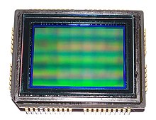
CCDs containing grids of pixels are used in digital cameras, optical scanners, and video cameras as light-sensing devices. They commonly respond to 70 per centum of the incident light (significant a quantum efficiency of about 70 percent) making them far more efficient than photographic film, which captures only about 2 percent of the incident light.
Nigh common types of CCDs are sensitive to most-infrared light, which allows infrared photography, dark-vision devices, and zilch lux (or most zippo lux) video-recording/photography. For normal silicon-based detectors, the sensitivity is limited to one.ane μm. One other effect of their sensitivity to infrared is that infrared from remote controls ofttimes appears on CCD-based digital cameras or camcorders if they practise not take infrared blockers.
Cooling reduces the array's night current, improving the sensitivity of the CCD to depression calorie-free intensities, even for ultraviolet and visible wavelengths. Professional observatories ofttimes cool their detectors with liquid nitrogen to reduce the night current, and therefore the thermal noise, to negligible levels.
Frame transfer CCD [edit]
A frame transfer CCD sensor
The frame transfer CCD imager was the first imaging structure proposed for CCD Imaging by Michael Tompsett at Bell Laboratories. A frame transfer CCD is a specialized CCD, often used in astronomy and some professional video cameras, designed for high exposure efficiency and correctness.
The normal functioning of a CCD, astronomical or otherwise, tin can be divided into two phases: exposure and readout. During the get-go phase, the CCD passively collects incoming photons, storing electrons in its cells. Afterwards the exposure time is passed, the cells are read out one line at a fourth dimension. During the readout stage, cells are shifted down the entire area of the CCD. While they are shifted, they continue to collect light. Thus, if the shifting is not fast enough, errors tin result from light that falls on a jail cell holding accuse during the transfer. These errors are referred to as "vertical smear" and crusade a strong light source to create a vertical line above and below its exact location. In addition, the CCD cannot be used to collect light while it is existence read out. Unfortunately, a faster shifting requires a faster readout, and a faster readout tin introduce errors in the cell accuse measurement, leading to a college noise level.
A frame transfer CCD solves both issues: it has a shielded, non light sensitive, area containing as many cells every bit the area exposed to light. Typically, this area is covered by a cogitating fabric such every bit aluminium. When the exposure time is up, the cells are transferred very chop-chop to the hidden expanse. Here, safe from any incoming light, cells can be read out at any speed one deems necessary to correctly measure the cells' charge. At the same time, the exposed office of the CCD is collecting low-cal once more, then no delay occurs betwixt successive exposures.
The disadvantage of such a CCD is the college toll: the cell area is basically doubled, and more complex control electronics are needed.
Intensified charge-coupled device [edit]
An intensified accuse-coupled device (ICCD) is a CCD that is optically connected to an image intensifier that is mounted in forepart of the CCD.
An image intensifier includes three functional elements: a photocathode, a micro-channel plate (MCP) and a phosphor screen. These iii elements are mounted one close behind the other in the mentioned sequence. The photons which are coming from the low-cal source fall onto the photocathode, thereby generating photoelectrons. The photoelectrons are accelerated towards the MCP by an electrical control voltage, practical between photocathode and MCP. The electrons are multiplied inside of the MCP and thereafter accelerated towards the phosphor screen. The phosphor screen finally converts the multiplied electrons dorsum to photons which are guided to the CCD past a fiber optic or a lens.
An epitome intensifier inherently includes a shutter functionality: If the control voltage between the photocathode and the MCP is reversed, the emitted photoelectrons are not accelerated towards the MCP but render to the photocathode. Thus, no electrons are multiplied and emitted by the MCP, no electrons are going to the phosphor screen and no calorie-free is emitted from the image intensifier. In this case no lite falls onto the CCD, which means that the shutter is closed. The process of reversing the control voltage at the photocathode is called gating and therefore ICCDs are also called gateable CCD cameras.
Besides the extremely high sensitivity of ICCD cameras, which enable single photon detection, the gateability is 1 of the major advantages of the ICCD over the EMCCD cameras. The highest performing ICCD cameras enable shutter times as brusque as 200 picoseconds.
ICCD cameras are in full general somewhat higher in cost than EMCCD cameras because they need the expensive prototype intensifier. On the other hand, EMCCD cameras need a cooling system to cool the EMCCD chip down to temperatures effectually 170 Thousand (−103 °C). This cooling organisation adds additional costs to the EMCCD photographic camera and often yields heavy condensation problems in the awarding.
ICCDs are used in night vision devices and in various scientific applications.
Electron-multiplying CCD [edit]
Electrons are transferred serially through the proceeds stages making up the multiplication register of an EMCCD. The loftier voltages used in these serial transfers induce the creation of additional charge carriers through impact ionisation.

in an EMCCD there is a dispersion (variation) in the number of electrons output by the multiplication annals for a given (stock-still) number of input electrons (shown in the legend on the right). The probability distribution for the number of output electrons is plotted logarithmically on the vertical axis for a simulation of a multiplication register. Also shown are results from the empirical fit equation shown on this page.
An electron-multiplying CCD (EMCCD, also known every bit an L3Vision CCD, a product commercialized past e2v Ltd., GB, L3CCD or Impactron CCD, a at present-discontinued production offered in the past past Texas Instruments) is a charge-coupled device in which a gain annals is placed between the shift annals and the output amplifier. The gain register is split up up into a large number of stages. In each stage, the electrons are multiplied past affect ionization in a similar way to an avalanche diode. The gain probability at every stage of the register is modest (P < 2%), but every bit the number of elements is large (N > 500), the overall gain can be very high ( ), with single input electrons giving many thousands of output electrons. Reading a point from a CCD gives a noise background, typically a few electrons. In an EMCCD, this noise is superimposed on many thousands of electrons rather than a single electron; the devices' master advantage is thus their negligible readout racket. The use of barrage breakup for distension of photograph charges had already been described in the U.S. Patent 3,761,744 in 1973 past George Due east. Smith/Bell Telephone Laboratories.

EMCCDs show a similar sensitivity to intensified CCDs (ICCDs). However, as with ICCDs, the proceeds that is applied in the gain register is stochastic and the verbal gain that has been applied to a pixel's accuse is impossible to know. At high gains (> 30), this uncertainty has the aforementioned issue on the bespeak-to-dissonance ratio (SNR) as halving the quantum efficiency (QE) with respect to functioning with a gain of unity. This effect is referred to as the Excess Noise Gene (ENF). However, at very low light levels (where the quantum efficiency is most important), it can be assumed that a pixel either contains an electron—or non. This removes the racket associated with the stochastic multiplication at the risk of counting multiple electrons in the aforementioned pixel as a single electron. To avoid multiple counts in one pixel due to ancillary photons in this way of performance, loftier frame rates are essential. The dispersion in the gain is shown in the graph on the right. For multiplication registers with many elements and big gains information technology is well modelled by the equation:

where P is the probability of getting n output electrons given g input electrons and a total mean multiplication register gain of g. For very big numbers of input electrons, this complex distribution function converges towards a Gaussian.
Because of the lower costs and better resolution, EMCCDs are capable of replacing ICCDs in many applications. ICCDs still have the advantage that they can be gated very fast and thus are useful in applications like range-gated imaging. EMCCD cameras indispensably need a cooling arrangement—using either thermoelectric cooling or liquid nitrogen—to absurd the fleck down to temperatures in the range of −65 to −95 °C (−85 to −139 °F). This cooling arrangement unfortunately adds additional costs to the EMCCD imaging system and may yield condensation problems in the application. However, loftier-finish EMCCD cameras are equipped with a permanent hermetic vacuum arrangement confining the chip to avoid condensation issues.
The low-calorie-free capabilities of EMCCDs observe use in astronomy and biomedical research, among other fields. In particular, their low dissonance at high readout speeds makes them very useful for a diversity of astronomical applications involving depression light sources and transient events such as lucky imaging of faint stars, high speed photon counting photometry, Fabry-Pérot spectroscopy and high-resolution spectroscopy. More recently, these types of CCDs have cleaved into the field of biomedical research in low-lite applications including small-scale brute imaging, single-molecule imaging, Raman spectroscopy, super resolution microscopy too equally a wide variety of modern fluorescence microscopy techniques thanks to greater SNR in low-light weather in comparison with traditional CCDs and ICCDs.
In terms of noise, commercial EMCCD cameras typically accept clock-induced charge (CIC) and dark current (dependent on the extent of cooling) that together lead to an effective readout noise ranging from 0.01 to 1 electrons per pixel read. However, recent improvements in EMCCD technology have led to a new generation of cameras capable of producing significantly less CIC, higher charge transfer efficiency and an EM gain 5 times higher than what was previously available. These advances in depression-light detection atomic number 82 to an effective total background noise of 0.001 electrons per pixel read, a noise flooring unmatched past any other low-lite imaging device.[25]
Utilise in astronomy [edit]

Due to the loftier quantum efficiencies of accuse-coupled device (CCD) (the ideal quantum efficiency is 100%, one generated electron per incident photon), linearity of their outputs, ease of use compared to photographic plates, and a variety of other reasons, CCDs were very speedily adopted by astronomers for nearly all UV-to-infrared applications.
Thermal noise and catholic rays may alter the pixels in the CCD array. To counter such effects, astronomers take several exposures with the CCD shutter airtight and opened. The average of images taken with the shutter closed is necessary to lower the random noise. One time adult, the dark frame average epitome is then subtracted from the open-shutter image to remove the dark current and other systematic defects (dead pixels, hot pixels, etc.) in the CCD. Newer Skipper CCDs counter dissonance past collecting data with the same collected accuse multiple times and has applications in precision light Dark Matter searches and neutrino measurements.[26] [27] [28]
The Hubble Infinite Telescope, in particular, has a highly developed series of steps ("data reduction pipeline") to convert the raw CCD data to useful images.[29]
CCD cameras used in astrophotography often require sturdy mounts to cope with vibrations from wind and other sources, along with the tremendous weight of most imaging platforms. To take long exposures of galaxies and nebulae, many astronomers employ a technique known as auto-guiding. Most autoguiders utilise a second CCD chip to monitor deviations during imaging. This chip can speedily notice errors in tracking and command the mount motors to correct for them.
An unusual astronomical application of CCDs, chosen drift-scanning, uses a CCD to make a fixed telescope conduct like a tracking telescope and follow the motility of the sky. The charges in the CCD are transferred and read in a direction parallel to the movement of the sky, and at the aforementioned speed. In this manner, the telescope tin image a larger region of the sky than its normal field of view. The Sloan Digital Heaven Survey is the most famous example of this, using the technique to produce a survey of over a quarter of the sky.
In addition to imagers, CCDs are also used in an array of belittling instrumentation including spectrometers[30] and interferometers.[31]
Color cameras [edit]
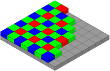
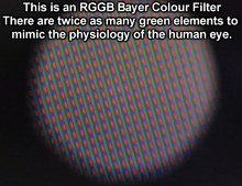
x80 microscope view of an RGGB Bayer filter on a 240 line Sony CCD PAL Camcorder CCD sensor
Digital color cameras generally use a Bayer mask over the CCD. Each foursquare of four pixels has one filtered red, 1 blue, and two green (the man heart is more sensitive to dark-green than either red or blue). The result of this is that luminance information is nerveless at every pixel, but the colour resolution is lower than the luminance resolution.
Better colour separation tin be reached by iii-CCD devices (3CCD) and a dichroic beam splitter prism, that splits the epitome into red, greenish and blue components. Each of the three CCDs is arranged to answer to a particular color. Many professional person video camcorders, and some semi-professional camcorders, utilize this technique, although developments in competing CMOS technology accept fabricated CMOS sensors, both with beam-splitters and bayer filters, increasingly popular in high-end video and digital cinema cameras. Another advantage of 3CCD over a Bayer mask device is higher quantum efficiency (higher light sensitivity), because almost of the light from the lens enters one of the silicon sensors, while a Bayer mask absorbs a high proportion (more than than two/3) of the light falling on each pixel location.
For nonetheless scenes, for instance in microscopy, the resolution of a Bayer mask device tin be enhanced by microscanning engineering science. During the procedure of colour co-site sampling, several frames of the scene are produced. Between acquisitions, the sensor is moved in pixel dimensions, then that each bespeak in the visual field is acquired consecutively by elements of the mask that are sensitive to the scarlet, green, and blue components of its colour. Somewhen every pixel in the prototype has been scanned at least once in each colour and the resolution of the iii channels go equivalent (the resolutions of cherry and bluish channels are quadrupled while the greenish aqueduct is doubled).
Sensor sizes [edit]
Sensors (CCD / CMOS) come in various sizes, or prototype sensor formats. These sizes are oft referred to with an inch fraction designation such as 1/one.8″ or two/3″ called the optical format. This measurement originates back in the 1950s and the time of Vidicon tubes.
Blooming [edit]
When a CCD exposure is long enough, somewhen the electrons that collect in the "bins" in the brightest part of the image will overflow the bin, resulting in blooming. The structure of the CCD allows the electrons to period more hands in ane direction than another, resulting in vertical streaking.[32] [33] [34]
Some anti-blooming features that can exist congenital into a CCD reduce its sensitivity to lite past using some of the pixel area for a drain construction.[35] James One thousand. Early developed a vertical anti-blooming drain that would not detract from the low-cal collection surface area, then did not reduce light sensitivity.
Meet also [edit]
- Photodiode
- CMOS sensor
- Bending-sensitive pixel
- Rotating line camera
- Superconducting camera
- Video camera tube – The prevailing video capture technology prior to the introduction of CCDs
- Wide dynamic range
- Pigsty accumulation diode (HAD)
- Multi-layer CCD
- Andor Technology – Manufacturer of EMCCD cameras
- Photometrics - Manufacturer of EMCCD cameras
- QImaging - Manufacturer of EMCCD cameras
- PI/Acton – Manufacturer of EMCCD cameras
- Time delay and integration (TDI)
- Glossary of video terms
- Category: Digital cameras with CCD image sensor
References [edit]
- ^ a b Sze, Simon Min; Lee, Ming-Kwei (May 2012). "MOS Capacitor and MOSFET". Semiconductor Devices: Physics and Technology. John Wiley & Sons. ISBN9780470537947 . Retrieved vi October 2019.
- ^ a b c d e f g h i Fossum, Due east. R.; Hondongwa, D. B. (2014). "A Review of the Pinned Photodiode for CCD and CMOS Epitome Sensors". IEEE Periodical of the Electron Devices Society. 2 (3): 33–43. doi:x.1109/JEDS.2014.2306412.
- ^ a b Williams, J. B. (2017). The Electronics Revolution: Inventing the Future. Springer. p. 245. ISBN9783319490885.
- ^ "1960: Metal Oxide Semiconductor (MOS) Transistor Demonstrated". The Silicon Engine. Reckoner History Museum. Retrieved Baronial 31, 2019.
- ^ James R. Janesick (2001). Scientific charge-coupled devices. SPIE Printing. p. iv. ISBN978-0-8194-3698-6.
- ^ See U.S. Patent 3,792,322 and U.S. Patent iii,796,927
- ^ W. Due south. Boyle; G. E. Smith (April 1970). "Charge Coupled Semiconductor Devices". Bell Syst. Tech. J. 49 (4): 587–593. doi:ten.1002/j.1538-7305.1970.tb01790.10.
- ^ Gilbert Frank Amelio; Michael Francis Tompsett; George East. Smith (April 1970). "Experimental Verification of the Charge Coupled Device Concept". Bell Syst. Tech. J. 49 (4): 593–600. doi:10.1002/j.1538-7305.1970.tb01791.x.
- ^ U.Due south. Patent four,085,456
- ^ M. F. Tompsett; G. F. Amelio; G. E. Smith (ane August 1970). "Charge Coupled viii-flake Shift Annals". Practical Physics Letters. 17 (3): 111–115. Bibcode:1970ApPhL..17..111T. doi:x.1063/one.1653327.
- ^ Tompsett, Yard.F.; Amelio, G.F.; Bertram, W.J. Jr.; Buckley, R.R.; McNamara, W.J.; Mikkelsen, J.C. Jr.; Sealer, D.A. (Nov 1971). "Charge-coupled imaging devices: Experimental results". IEEE Transactions on Electron Devices. xviii (eleven): 992–996. Bibcode:1971ITED...eighteen..992T. doi:10.1109/T-ED.1971.17321. ISSN 0018-9383.
- ^ Dobbin, Ben (8 September 2005). "Kodak engineer had revolutionary idea: the showtime digital photographic camera". Seattle Postal service-Intelligencer. Archived from the original on 25 January 2012. Retrieved 2011-11-xv .
- ^ globalsecurity.org - KH-eleven KENNAN, 2007-04-24
- ^ "NRO review and redaction guide (2006 ed.)" (PDF). National Reconnaissance Part.
- ^ Johnstone, B. (1999). Nosotros Were Burning: Japanese Entrepreneurs and the Forging of the Electronic Historic period. New York: Bones Books. ISBN0-465-09117-2.
- ^ Hagiwara, Yoshiaki (2001). "Microminiaturization for Home Amusement". In Oklobdzija, Vojin Thou. (ed.). The Computer Applied science Handbook. CRC Printing. p. 41-vi. ISBN978-0-8493-0885-7.
- ^ U.Due south. Patent 4,484,210: Solid-land imaging device having a reduced epitome lag
- ^ Teranishi, Nobuzaku; Kohono, A.; Ishihara, Yasuo; Oda, E.; Arai, 1000. (December 1982). "No image lag photodiode structure in the interline CCD image sensor". 1982 International Electron Devices Coming together: 324–327. doi:10.1109/IEDM.1982.190285. S2CID 44669969.
- ^ "Charles Stark Draper Award". Archived from the original on 2007-12-28.
- ^ "Nobel Prize website".
- ^ Gilbert F. Amelio (February 1974). "Charge-Coupled Devices". Scientific American. 230 (ii).
- ^ For instance, the specsheet of PI/Acton'southward SPEC-ten camera specifies a dark current of 0.3 electron per pixel per 60 minutes at −110 °C (−166 °F).
- ^ a b c Sze, S. M.; Ng, Kwok K. (2007). Physics of semiconductor devices (3 ed.). John Wiley and Sons. ISBN978-0-471-14323-9. Chapter 13.6.
- ^ Apogee CCD Academy - Pixel Binning [ permanent dead link ]
- ^ Daigle, Olivier; Djazovski, Oleg; Laurin, Denis; Doyon, René; Artigau, Étienne (July 2012). "Characterization results of EMCCDs for extreme low calorie-free imaging" (PDF).
- ^ Aguilar-Arevalo, A.; Amidei, D.; Baxter, D.; Cancelo, G.; Vergara, B. A. Cervantes; Chavarria, A. E.; Darragh-Ford, E.; Neto, J. R. T. de Mello; D'Olivo, J. C.; Estrada, J.; Gaïor, R. (2019-10-31). "Constraints on Light Dark Matter Particles Interacting with Electrons from DAMIC at SNOLAB". Physical Review Letters. 123 (18): 181802. arXiv:1907.12628. Bibcode:2019PhRvL.123r1802A. doi:10.1103/PhysRevLett.123.181802. ISSN 0031-9007. PMID 31763884. S2CID 198985735.
- ^ Abramoff, Orr. "Skipper CCD". SENSEI . Retrieved xi Apr 2021.
- ^ Aguilar-Arevalo, Alexis; Bertou, Xavier; Bonifazi, Carla; Cancelo, Gustavo; Castañeda, Alejandro; Vergara, Brenda Cervantes; Chavez, Claudio; D'Olivo, Juan C.; Anjos, João C. dos; Estrada, Juan; Neto, Aldo R. Fernandes (2019-xi-13). "Exploring depression-energy neutrino physics with the Coherent Neutrino Nucleus Interaction Experiment (CONNIE)". Concrete Review D. 100 (ix): 092005. arXiv:1906.02200. doi:10.1103/PhysRevD.100.092005. hdl:11336/123886. ISSN 2470-0010. S2CID 174802422.
- ^ Hainaut, Oliver R. (Dec 2006). "Basic CCD image processing". Retrieved January xv, 2011.
Hainaut, Oliver R. (June 1, 2005). "Signal, Racket and Detection". Retrieved October 7, 2009.
Hainaut, Oliver R. (May 20, 2009). "Retouching of astronomical data for the product of outreach images". Retrieved October 7, 2009.
(Hainaut is an astronomer at the European Southern Observatory)
- ^ Deckert, Five.; Kiefer, W. (1992). "Scanning multichannel technique for improved spectrochemical measurements with a CCD camera and its application to Raman spectroscopy". Appl. Spectrosc. 46 (2): 322–328. Bibcode:1992ApSpe..46..322D. doi:10.1366/0003702924125500. S2CID 95441651.
- ^ Duarte, F. J. (1993). "On a generalized interference equation and interferometric measurements". Opt. Commun. 103 (1–2): 8–xiv. Bibcode:1993OptCo.103....8D. doi:10.1016/0030-4018(93)90634-H.
- ^ Phil Plait. "The Planet Ten Saga: SOHO Images"
- ^ Phil Plait. "Why, Male monarch Triton, how nice to see you!"
- ^ Thomas J. Fellers and Michael W. Davidson. "CCD Saturation and Blooming" Archived July 27, 2012, at the Wayback Auto
- ^ Albert J. P. Theuwissen (1995). Solid-Land Imaging With Charge-Coupled Devices. Springer. pp. 177–180. ISBN9780792334569.
External links [edit]
- Journal Article On Nuts of CCDs
- Nikon microscopy introduction to CCDs
- Concepts in Digital Imaging Applied science
- More statistical properties
- L3CCDs used in astronomy
Source: https://en.wikipedia.org/wiki/Charge-coupled_device
Posted by: markshowere.blogspot.com
0 Response to "Which Cameras Use Ccd Sensor"
Post a Comment